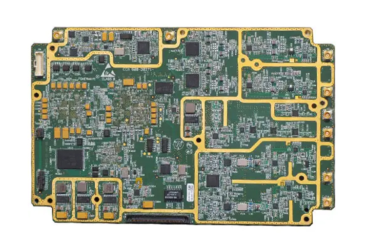
CAPABILITIES IN military pcb assembly
Military Grade PCB assembly need to be robust enough to comply with the harsh conditions it needs to function in. That calls for the following:
SpecifIC layout techniques
100% design-for-test coverage
Thermal Management
rigid PCBs, flex PCBs, Rigid Flex PCBs, and single sided PCBs, and double-sided PCBs
multilayer PCBs.
At Technotronix, we are fully equipped to provide these. In addition, all the components that we use measure up to military specs. These components have low tolerance range. Also, the design of the Military PCB handles maximum current load and works uninterrupted in harsh environments. In our layouts, we ensure the following:
Right aspect ratios
Separating power and ground planes
Keeping signals clean
Verifying impedance calculations
Performing pre layout SIMulations
Adequate termination techniques
Exact drill charts and proper board materials
We are fully committed to offer state-of-the-art prototype and production services for the defense and military industry.
Our robust testing standards as well as our industry certifications stand testimony to the quality we offer.

APPLICATIONS OF MILITARY GRADE circuit boards
Military Grade printed circuit boards Assembly finds wide application in an array of areas including but not limited to:
Military Robotic Systems
Defense communication and navigation
Ruggedized Computers
Power Distribution
Base/CAMp protection and security
circuit board Schematic and layout
Artillery and Mortars
Unmanned vehicles
Turnkey product assembly


